
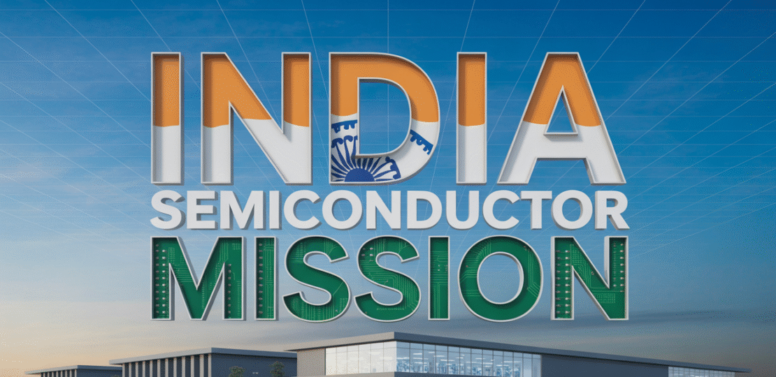
India Semiconductor Mission – The Game-Changer For Digital Future
September 5, 2025 | by support@rabgcontent.com
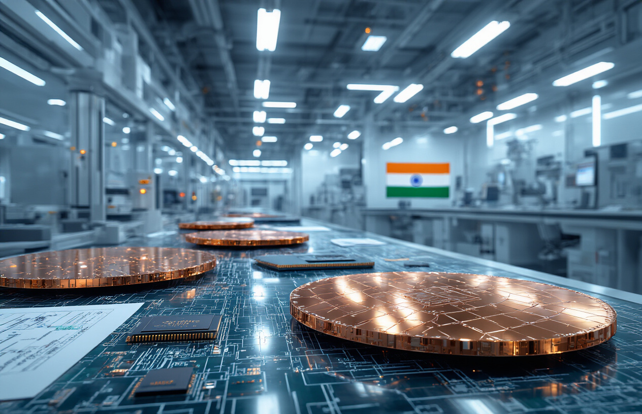
The India Semiconductor Mission is transforming the country from a chip importer into a serious player in global semiconductor manufacturing. This government initiative, launched in 2021, targets tech professionals, investors, policymakers, and business leaders interested in India’s rapidly growing chip industry.
ISM has already approved $13+ billion in projects across ten major facilities, from Tata’s massive fab investment to Micron’s assembly plant in Gujarat. This comprehensive program offers up to 50% fiscal support for approved projects, making India an attractive alternative to traditional manufacturing hubs.
We’ll explore three key areas that showcase India’s strategic approach. First, we’ll examine the government support schemes driving industry growth and how they stack up against global competitors. Second, we’ll dive into major investment milestones and approved projects that are reshaping India’s tech landscape. Finally, we’ll look at how states like Gujarat are building specialized semiconductor clusters and infrastructure advantages that position India as a trusted partner in the global supply chain.
Unlike China’s inward-focused strategy, India is actively courting international partnerships while building domestic capabilities. This balanced approach is already attracting record investments and establishing India as a key player in semiconductor manufacturing.
Understanding India’s Semiconductor Mission and Its Strategic Vision
Understanding India’s Semiconductor Mission and Its Strategic Vision
The India Semiconductor Mission represents a transformative initiative launched in 2021 that aims to position the nation at the forefront of global semiconductor manufacturing and innovation. This ambitious program has rapidly evolved from vision to reality, with the government announcing a substantial ₹76,000 crore Production Linked Incentive (PLI) scheme, of which nearly ₹65,000 crore has already been committed to various projects across the semiconductor value chain.
Building a Vibrant Semiconductor and Display Ecosystem
The India Semiconductor Mission’s primary objective centers on creating a comprehensive semiconductor and display ecosystem that encompasses the entire value chain. This ecosystem approach includes establishing chip manufacturing plants (fabs), creating packaging and testing units, supporting startups in chip design, and training young engineers to build a skilled workforce for the industry.
The mission’s strategic vision extends beyond mere manufacturing to include cutting-edge research in semiconductors and display technology, including both evolutionary and revolutionary technologies through grants, global collaborations, and other mechanisms in academia, research institutions, and industry. This comprehensive approach enables the establishment of Centers of Excellence (CoEs) that drive innovation and technological advancement.
India’s capacity to emerge as a key contributor spans three primary pillars of the semiconductor manufacturing supply chain: Equipment – leveraging the strong base of MSMEs to produce components for semiconductor equipment; Materials – utilizing India’s rich sources of chemicals, minerals, and gases; and Services – capitalizing on major talent in AI, big data, cloud computing, and IoT for R&D, logistics, and supply chain management.
Positioning India as a Global Electronics Manufacturing Hub
With the global semiconductor market expected to reach USD 1 trillion by 2030, the India Semiconductor Mission strategically positions the country to capture a substantial portion of this expanding market. The mission facilitates the adoption of secure microelectronics and developing trusted semiconductor supply chains, including raw materials, specialty chemicals, gases, and manufacturing equipment.
The initiative has already achieved remarkable milestones, with 10 approved semiconductor projects across six states representing an investment of ₹1.60 lakh crore. These projects position India to compete shoulder-to-shoulder with global leaders in semiconductor manufacturing. Notable achievements include India’s first commercial Silicon Carbide fab in Odisha and advanced packaging units bringing next-generation technologies to fulfill the nation’s semiconductor ambitions.
The mission’s focus on advanced technology development is evident in recent breakthroughs, including the inauguration of two state-of-the-art semiconductor design facilities in Noida and Bengaluru in May 2025. These centers represent India’s first facilities focused on advanced 3-nanometer chip design, marking a significant milestone in the nation’s semiconductor innovation journey and demonstrating the country’s progression from 7nm and 5nm designs to cutting-edge 3nm technology.
Serving as the Nodal Agency for Seamless Implementation
As the central coordinating body, the India Semiconductor Mission serves as the nodal agency for the efficient and seamless implementation of semiconductor and display schemes. The mission is envisioned to be led by global experts in the semiconductor and display industry, ensuring world-class execution and strategic oversight of all initiatives.
The mission’s implementation strategy includes formulating long-term strategies for developing sustainable semiconductors and display manufacturing facilities and semiconductor design ecosystems in the country. It enables multi-fold growth of Indian semiconductor design industry by providing requisite support in the form of Electronic Design Automation (EDA) tools, foundry services, and other suitable mechanisms for early-stage startups.
Through the Design Linked Incentive (DLI) scheme, 23 chip design projects have been sanctioned to support startups and innovators, with companies like Vervesemi Microelectronics creating advanced chips for defense, aerospace, electric vehicles, and energy systems. This demonstrates India’s evolution from being merely a consumer to becoming a creator in the semiconductor industry.
The mission also promotes and facilitates indigenous Intellectual Property (IP) generation while encouraging Transfer of Technologies (ToT) through collaboration and partnership programs with national and international agencies, industries, and institutions for catalyzing collaborative research, commercialization, and skill development.
Government Support Schemes Driving Industry Growth

Government Support Schemes Driving Industry Growth
The India Semiconductor Mission has structured comprehensive incentive programs to accelerate domestic semiconductor manufacturing through strategic financial support across multiple segments of the value chain.
Semiconductor Fabs scheme offering 50% fiscal support
The flagship Semiconductor Fabs scheme represents the government’s most ambitious commitment to establishing advanced chip manufacturing capabilities in India. This program extends fiscal support of up to 50% of project cost on a pari-passu basis to approved applicants, ensuring immediate upfront funding availability rather than post-completion reimbursements.
The scheme operates under strict oversight, with the Expenditure Finance Committee chaired by the Secretary of the Department of Expenditure determining both the structure and quantum of fiscal support for each semiconductor fab project. To qualify, companies must meet substantial investment thresholds of INR 200 billion, demonstrate revenue capabilities of INR 75 billion, and commit to 300mm wafer size technology with minimum capacity of 40,000 wafer starts per month.
This pari-passu funding model deposits subsidies into dedicated “No-Lien Accounts” created by beneficiaries, enabling real-time fund tracking while preventing diversion to non-project purposes. The disbursement occurs in instalments, beginning after beneficiaries mobilize their funding share and continuing based on submitted project reports until full fiscal support is provided.
Display Fabs incentive program structure
With this comprehensive semiconductor support framework in mind, the Display Fabs scheme mirrors the semiconductor program’s structure while targeting display manufacturing capabilities. The initiative extends identical 50% fiscal support on a pari-passu basis, maintaining the same rigorous oversight through the Expenditure Finance Committee.
Display manufacturing projects require INR 100 billion minimum investment with INR 75 billion revenue thresholds. Technical specifications demand Generation 8 or above technology for TFT LCD facilities or Generation 6 or above for AMOLED manufacturing, with corresponding monthly capacity requirements of 60,000 panels for TFT LCD or 30,000 panels for AMOLED production.
The program follows identical accountability measures, requiring quarterly review reports, three-year production maintenance commitments post-commercial operations, and six-year project completion timelines from approval dates.
Design Linked Incentive scheme for IC development
Now that we have covered manufacturing infrastructure support, the Design Linked Incentive (DLI) scheme addresses the critical design ecosystem development over a five-year implementation period. This program offers financial incentives alongside design infrastructure support across various development and deployment stages for semiconductor designs.
The scheme encompasses Integrated Circuits (ICs), Chipsets, System on Chips (SoCs), Systems & IP Cores, and semiconductor-linked designs. Rather than focusing solely on manufacturing capabilities, the DLI program builds India’s design competencies essential for creating proprietary semiconductor solutions and establishing the country as a trusted partner in global semiconductor supply chains.
Compound semiconductors and packaging facility support
Previously established manufacturing schemes primarily targeted traditional silicon-based semiconductors. The compound semiconductors scheme extends 50% capital expenditure support to specialized manufacturing facilities including Silicon Photonics, Sensors (including MEMS), Discrete Semiconductors Fabs, and Semiconductor ATMP/OSAT facilities.
This targeted support addresses emerging technology segments with lower investment barriers of INR 500 million for ATMP/OSAT units, requiring 150/200mm or larger wafer processing capabilities with minimum 500 wafer starts monthly capacity. The compound semiconductor facilities represent strategic positioning in advanced packaging and specialized semiconductor applications, enabling India to participate in high-value segments of the global semiconductor ecosystem.
These comprehensive government support schemes demonstrate India’s commitment to building end-to-end semiconductor manufacturing capabilities while providing substantial financial backing to attract global industry leaders and establish domestic production capacity across the entire semiconductor value chain.
Major Investment Milestones and Approved Projects

Major Investment Milestones and Approved Projects
Tata Electronics’ $10 billion fab investment breakthrough
Tata Electronics has emerged as a cornerstone of India’s semiconductor manufacturing ambitions with its groundbreaking $10.37 billion investment in partnership with Taiwan’s Powerchip Semiconductor Manufacturing Corp (PSMC). This massive semiconductor fabrication facility, approved in February 2024, represents one of the largest single investments in India’s semiconductor industry.
Located in Dholera, Gujarat, this state-of-the-art facility will have an impressive output capacity of 50,000 wafers per month once fully operational. The project has already reached a significant milestone with the signing of the Foundry Services Agreement (FSA) between India Semiconductor Mission, Tata Electronics Private Limited, and Tata Semiconductor Manufacturing Private Limited in 2025.
This investment positions Tata Electronics as a major player in India’s semiconductor ecosystem and demonstrates the country’s capability to attract world-class manufacturing partnerships. The facility will serve diverse sectors including telecommunications, automotive, and consumer electronics, significantly reducing India’s dependency on semiconductor imports.
Micron Technology’s $2.75 billion ATMP plant establishment
Micron Technology made history as one of the first major international semiconductor companies to establish operations under the India Semiconductor Mission. The company’s $2.56 billion Assembly, Test, Mark, and Pack (ATMP) facility in Sanand, Gujarat, received approval in June 2023, marking a pivotal moment for semiconductor investment India.
This facility represents a strategic win for India’s semiconductor manufacturing capabilities, focusing on advanced packaging technologies. The plant will operate with a phased ramp-up approach, gradually increasing production capacity to meet both domestic and global demand. Micron’s investment demonstrates international confidence in India’s semiconductor mission government schemes and the country’s potential as a trusted manufacturing partner.
The ATMP facility will play a crucial role in the global semiconductor supply chain, positioning India as a key player in advanced packaging and testing operations.
Recent cabinet approval of four new semiconductor projects
The momentum in India semiconductor industry growth accelerated significantly with the Union Cabinet’s approval of four new semiconductor projects on August 12, 2025. These projects, worth approximately $524.39 million, represent a diverse portfolio of advanced manufacturing capabilities across multiple states.
SiCSem Private Limited will establish India’s first commercial Silicon Carbide (SiC) compound semiconductor fabrication facility in Bhubaneswar, Odisha, in collaboration with UK-based Clas-SiC Wafer Fab Ltd. This facility will produce 60,000 wafers annually and package 96 million units, addressing the growing demand for power electronics and electric vehicle applications.
Continental Device India Private Limited (CDIL) will expand its operations in Mohali, Punjab, focusing on high-power discrete semiconductor devices including MOSFETs, IGBTs, and Schottky Bypass Diodes using both silicon and silicon carbide technologies.
3D Glass Solutions Inc. will establish an advanced packaging facility in Odisha, utilizing cutting-edge technologies such as glass interposers, silicon bridges, and 3D Heterogeneous Integration modules.
Advanced System in Package (ASIP) Technologies will build a facility in Andhra Pradesh in partnership with South Korea’s APACT Co. Ltd., with an annual capacity of 96 million units serving multiple electronics applications.
Record-breaking startup investments and funding attraction
India’s semiconductor startup ecosystem has witnessed unprecedented growth, driven by robust government support and increasing investor confidence. The Design Linked Incentive Scheme has extended infrastructure support to 278 academic institutions and 72 startups, creating a vibrant innovation ecosystem.
In July 2025, MeitY approved 23 chip design projects from startups, MSMEs, and academic institutions, focusing on applications including surveillance systems, smart meters, networking equipment, and microprocessor IP cores. This demonstrates the comprehensive approach of India Semiconductor Mission in nurturing both manufacturing and design capabilities.
The scheme’s impact is already visible with 10 startups securing venture capital funding, six companies completing prototype tape-outs at international foundries, and 17 institutions fabricating 20 chip designs at the semiconductor laboratory in Mohali, Punjab. The sanctioned outlay has reached INR 8.03 billion, offering up to 50 percent cost coverage for design and prototyping activities.
With this comprehensive investment portfolio totaling approximately $18.23 billion across 10 sanctioned projects, India has established itself as a serious contender in the global semiconductor manufacturing landscape, attracting both domestic and international players to participate in its ambitious semiconductor mission.
India’s Strategic Approach Versus Global Competition

India’s Strategic Approach Versus Global Competition
Collaborative Model with International Anchor Firms
India’s semiconductor strategy fundamentally differs from other nations through its emphasis on collaborative partnerships with international anchor firms. Rather than pursuing a purely domestic approach, India has adopted a model that actively solicits interest from key global semiconductor companies, particularly those based in the United States and Europe. This collaborative framework brings significant advantages beyond just the anchor firm itself—it enables entire supplier ecosystems to relocate alongside these major players.
The success of this approach is exemplified by Micron Technology’s $2.75 billion investment in Gujarat, which brought with it an entire network of suppliers, subsuppliers, and other industry players to India. This cascading effect demonstrates how attracting one major international player can catalyze broader ecosystem development. The approach mirrors India’s success in other sectors, such as incentivizing Apple to move substantial assembly operations and its supplier ecosystem to India, with similar efforts being made to attract Tesla and electric vehicle manufacturers.
This collaborative model allows India to leverage existing global expertise while building domestic capabilities, creating a more integrated approach to semiconductor development than purely indigenous strategies might achieve.
Contrasting Approach with China’s Inward-Looking Strategy
The contrast between India’s collaborative approach and China’s semiconductor strategy is particularly notable. While China has devoted considerably more capital toward its semiconductor journey, its approach has been characterized as more “inward-looking,” driven primarily by the quest to accelerate self-reliance rather than working with the best semiconductor firms in the global market. China’s motivations stem from pursuing technological self-reliance, responding to U.S. export controls, and the desire to “design out” American components from its supply chains.
China’s strategy involves undertaking the ambitious task of building its own version of technologies that currently serve as chokepoints in the semiconductor supply chain. Despite deploying larger scale funds, China’s results have been mixed when considering the overall capital invested. This inward-focused approach contrasts sharply with India’s strategy of encouraging domestic firms to invest in nascent semiconductor hubs while simultaneously attracting international anchor firms.
India’s approach recognizes that in the complex semiconductor industry, collaboration often yields better results than complete self-reliance, particularly when building capabilities from a relatively early stage in the development cycle.
Leveraging Global Supply Chain Shifts and Trade Dynamics
India’s semiconductor mission has been significantly aided by larger shifts in global commerce and trade dynamics. According to World Bank data, India ranked among the top six economies that benefited from U.S. trade policy measures in terms of supply chain onshoring. This positioning is particularly impressive given that most countries ranking ahead of India were economies already well-integrated into global value chains, such as Vietnam, which was already part of trade agreements like the Regional Comprehensive Economic Partnership (RCEP).
The global trade environment has created opportunities that India has effectively capitalized upon. While U.S.-China trade growth was 30 percent slower than the two countries’ trade with other partners, economies like Vietnam experienced export surges to the United States. However, India’s advances in semiconductor investments are particularly noteworthy because they represent genuine capability building rather than merely serving as conduits for stretched supply chains.
Recent analysis by Moody’s highlights how India has performed well alongside countries like Malaysia and Singapore in attracting new global investments for semiconductor projects. The announcement of the new Electronics Component Manufacturing Scheme in April 2025 is expected to drive further upstream semiconductor investments, creating a virtuous cycle of ecosystem development.
Building Partnerships Without Major Multilateral Trade Agreements
India’s semiconductor success becomes even more remarkable when considering that it has achieved these advances without being part of major multilateral trade agreements like the RCEP or the Comprehensive and Progressive Agreement for Trans-Pacific Partnership. This demonstrates the effectiveness of India’s bilateral approach and targeted incentive structures in attracting global semiconductor investments.
Unlike countries that benefit from preferential trade arrangements and established regional value chains, India has had to build its semiconductor ecosystem through direct government initiatives, strategic partnerships, and competitive incentive schemes. The India Semiconductor Mission has successfully created a framework that attracts international players while fostering domestic capabilities, proving that effective policy implementation can overcome the absence of formal trade agreement advantages.
This approach has enabled India to participate meaningfully in global supply chain restructuring without relying on multilateral frameworks, instead building partnerships through targeted industry engagement and comprehensive government support schemes that address the specific needs of semiconductor manufacturers and their ecosystems.
State Competition and Gujarat’s Emerging Leadership

State Competition and Gujarat’s Emerging Leadership
Federal-state coordination process for project approvals
Gujarat’s semiconductor success stems from its strategic alignment with the Centre’s India Semiconductor Mission (ISM), creating a seamless dual-layered incentive structure. This coordination has enabled companies to access combined financial support of up to 70% capital subsidy—50% from the Government of India and an additional 20% from the state government. The Gujarat State Electronics Mission (GSEM) serves as the central coordinating body, facilitating expedited approvals through streamlined administrative processes. A remarkable example of this efficiency was demonstrated when Tata Electronics’ fabrication unit approval was granted within 24 hours, showcasing the state’s commitment to rapid project facilitation and its ability to work in tandem with federal initiatives.
Inter-state competition for additional investment incentives
With this coordinated approach in mind, Gujarat has positioned itself as one of the most financially competitive destinations globally for semiconductor investment. The state has attracted investment commitments exceeding ₹1.25 lakh crore from major companies including Tata Electronics, Micron Technology, CG Power, and Kaynes Semicon. Beyond the substantial capital subsidies, Gujarat offers comprehensive operational support including subsidized land allocation (up to 75% discount for the first 200 acres in Dholera), reduced utility tariffs, complete exemptions on stamp duty, and expedited approval mechanisms. This comprehensive incentive package has given Gujarat a significant competitive advantage over other states vying for semiconductor manufacturing investments.
Gujarat’s dedicated semiconductor policy advantages
The Gujarat Semiconductor Policy 2022-2027 represents a focused strategic initiative specifically designed to guide a significant portion of ISM investments to the state. This policy facilitates eligible projects through expedited land allotment, streamlined process approvals, and ready access to essential utilities including power, water, gas, and industrial infrastructure. The policy leverages Gujarat’s existing industrial advantages, including robust infrastructure, extensive network connectivity through National Highways and State Highways, 48 ports, 17 operational airports with 2 international facilities, and premier educational institutions. The presence of multiple specialized industrial zones under the Gujarat Industrial Development Corporation (GIDC) further strengthens the state’s positioning as an ideal semiconductor manufacturing hub.
Dholera Special Investment Region as a game-changing cluster
Previously established infrastructure investments now position Dholera Special Investment Region (DSIR) as the cornerstone of Gujarat’s semiconductor manufacturing strategy. Located strategically along the Delhi-Mumbai Industrial Corridor and near an upcoming international airport, Dholera is being developed as a specialized hub for chip fabrication activities. Tata Electronics is constructing what will be India’s first commercial semiconductor fabrication facility within DSIR, with operations expected to commence by 2027-28. The region’s development focuses on creating logistical synergies and promoting shared infrastructure to reduce operational costs and project timelines. This clustering approach extends beyond primary manufacturing to include the development of ancillary industries such as specialty gases, chemicals, and cleanroom technologies, creating a comprehensive ecosystem that reduces import reliance and improves supply chain resilience for semiconductor manufacturing operations.
Building Industrial Clusters and Infrastructure Advantages

Building Industrial Clusters and Infrastructure Advantages
Proximity to Major Ports and Transportation Networks
Gujarat’s Dholera Special Investment Region (Dholera SIR) has emerged as a strategic semiconductor hub primarily due to its exceptional logistical advantages. Standing at about 900 square kilometers, this dedicated industrial city benefits from proximity to two major ports within Gujarat alone, providing crucial access to global supply chains and export markets. This transportation infrastructure advantage sets Dholera SIR apart from other competing semiconductor investment destinations across India.
The cluster approach recognizes that semiconductor manufacturing requires seamless movement of materials, components, and finished products across international borders. With the semiconductor industry being inherently global, having direct access to major ports significantly reduces logistics costs and delivery times, making Gujarat’s offerings more attractive to international investors compared to landlocked alternatives.
Micron Investment Creating Catalyzing Supplier Ecosystem Effects
Micron Technology’s 2023 investment in Gujarat’s semiconductor ecosystem has served as a transformative catalyst for the region’s development. Even though heavily subsidized by both the Indian government and the State of Gujarat, this $2.75 billion cumulative investment brought more than just manufacturing capacity—it delivered an entire ecosystem of suppliers, subsuppliers, and supporting players to India.
The Micron investment has created powerful demonstration effects, validating India’s semiconductor environment as ready for business. This anchor firm approach aligns with India’s broader strategy of soliciting interest from key American companies to relocate operations, bringing their larger supplier ecosystems along with them. The proximity of these suppliers and contractors within the cluster reduces costs and accelerates innovation cycles, creating the knowledge spillovers essential for a thriving semiconductor ecosystem.
Effective Project Execution Over Financial Incentives Alone
Analysis of state-level competition reveals that financial incentives alone do not determine the overall attractiveness of semiconductor investment destinations. Gujarat’s success demonstrates that effective project execution and swift implementation often matter more than the highest subsidy rates. Despite offering “additional capital assistance” at 40 percent of the capex assistance given by the Government of India—less than the 50 percent capex financial support offered by Tamil Nadu, Odisha, Karnataka, and Andhra Pradesh—Gujarat has attracted the most significant investments.
This pattern becomes clear when comparing outcomes across states. Uttar Pradesh, despite being the only Indian state to provide “an overall ceiling of 100 percent of the total eligible project cost approved by the Government of India” under its semiconductor policy, has failed to generate interest from any major semiconductor firms. Similarly, Karnataka signed an MOU in 2022 with a consortium including Tower Semiconductor for a proposed $3 billion investment that ultimately did not materialize, highlighting that execution capabilities and business environment often trump pure financial incentives.
Brownfield Versus Greenfield Cluster Development Strategies
The reference content highlights a crucial distinction between Gujarat’s greenfield approach and other states’ brownfield strategies. Karnataka, Tamil Nadu, and Andhra Pradesh are competing with bespoke clusters for electronic and automotive manufacturing, but these represent brownfield clusters that are not specifically focused on semiconductors and lack the dedicated scale of a Dholera SIR.
Gujarat’s greenfield approach with Dholera SIR represents a purpose-built semiconductor ecosystem designed from the ground up. This dedicated semiconductor policy focus—Gujarat was the first state to introduce such specialized policy—creates concentrated infrastructure, shared facilities like power, cleanrooms, logistics, and testing capabilities specifically optimized for chip manufacturing. The greenfield model allows for better planning of supplier networks, talent pipelines through aligned universities and skill centers, and the creation of knowledge spillovers that occur when engineers and researchers operate within a dense, specialized ecosystem.
This strategic difference in cluster development approaches explains why Gujarat has successfully attracted major anchor investments while other states with competitive financial incentives have struggled to convert policy frameworks into actual manufacturing facilities.
Future Opportunities in Advanced Technology Development

Future Opportunities in Advanced Technology Development
Now that we have covered India’s strategic positioning in the global semiconductor landscape, the future opportunities in India’s advanced technology development present unprecedented potential for establishing the nation as a leader in cutting-edge semiconductor innovation.
Creating Intellectual Property for Novel End-Products
India’s focus on building indigenous intellectual property represents a cornerstone of its semiconductor strategy. The country is actively working to develop proprietary chip design capabilities and technical standards that will strengthen India’s position in the global semiconductor value chain. This initiative aims to reduce dependence on foreign technology while creating unique solutions tailored to domestic and international markets.
The development of indigenous design and standards encompasses comprehensive intellectual property creation across various semiconductor applications. With significant government support through initiatives like the INR 760 billion Semiconductor and Display Scheme, over 45 applications from startups and established companies are being evaluated to foster innovation in design, fabrication, and testing. This ecosystem development is crucial for creating novel end-products that address specific market needs while building India’s technological sovereignty.
Developing Next-Generation Medical Diagnostic Devices
The semiconductor sector’s expansion into healthcare applications presents substantial opportunities for India’s advanced technology development. With the growing demand for sophisticated medical diagnostic equipment, India’s semiconductor capabilities are positioning the country to develop next-generation medical devices that leverage advanced chip technologies.
The focus on AI-enabled chip manufacturing and MLOps initiatives, including the India AI program’s GPU cluster, creates a foundation for developing smart medical diagnostic devices. These technologies can enable more precise, faster, and cost-effective healthcare solutions, contributing to India’s growing reputation as a technology innovation hub.
Limited Focus on Electronic Design Automation Tools
While India’s semiconductor mission encompasses broad technological development, the reference materials indicate limited specific emphasis on electronic design automation (EDA) tools development. However, the establishment of R&D collaborations, such as AMD’s research center in Bengaluru, suggests potential for future expansion into EDA tool development as the semiconductor ecosystem matures.
The current focus remains primarily on manufacturing capabilities, infrastructure development, and design services rather than specialized EDA tool creation. This represents an area where future policy iterations could address gaps in the semiconductor value chain.
Leveraging India’s 20% Global Chip Design Workforce Potential
India’s substantial chip design workforce represents one of its most significant competitive advantages in the global semiconductor landscape. The planned expansion of chip design and R&D centers indicates strategic recognition of this human capital asset. With initiatives focusing on AI and high-performance computing sectors, India is positioned to capitalize on its design expertise to capture larger portions of the global semiconductor value chain.
The development of training centers and R&D collaborations supports the cultivation of this workforce potential. Investment in MLOps and AI-enabled chip manufacturing further enhances the capability of India’s design professionals to work on next-generation semiconductor technologies. This workforce advantage, combined with government incentives and infrastructure development, creates a foundation for sustained growth in advanced technology development across the semiconductor sector.

India’s semiconductor mission represents a remarkable transformation from scattered past attempts to a focused, strategic approach that has yielded tangible results in just four years. With ten approved projects worth billions in investment, including major commitments from Tata Electronics and Micron Technology, the India Semiconductor Mission has successfully positioned the country as an attractive destination for global semiconductor manufacturers. The strategic focus on building complete ecosystems rather than isolated facilities, combined with competitive state-level incentives and world-class infrastructure development, has created a foundation for sustained growth.
The mission’s India semiconductor Mission success lies not just in attracting investments, but in fostering a collaborative approach with international partners while nurturing domestic capabilities. As Gujarat emerges as the frontrunner with its dedicated semiconductor clusters and infrastructure advantages, other states continue to innovate their offerings, creating healthy competition that benefits the entire ecosystem. Looking ahead, India’s semiconductor journey must focus on advancing up the value chain through indigenous IP development and next-generation technology research, ensuring the country evolves from a manufacturing hub to an innovation leader in the global semiconductor landscape.
RELATED POSTS
View all

Apple 2025 MacBook Air 13-inch laptop with M4 chip: It’s Amazing
September 19, 2025 | by support@rabgcontent.com

What are the AI automation benefits? The Ultimate Guide
September 3, 2025 | by support@rabgcontent.com

Kya Aap Jante Hai Zoho Ka Hidden Truth ? 90% लोग इसका सही उपयोग नहीं करते!
October 7, 2025 | by support@rabgcontent.com